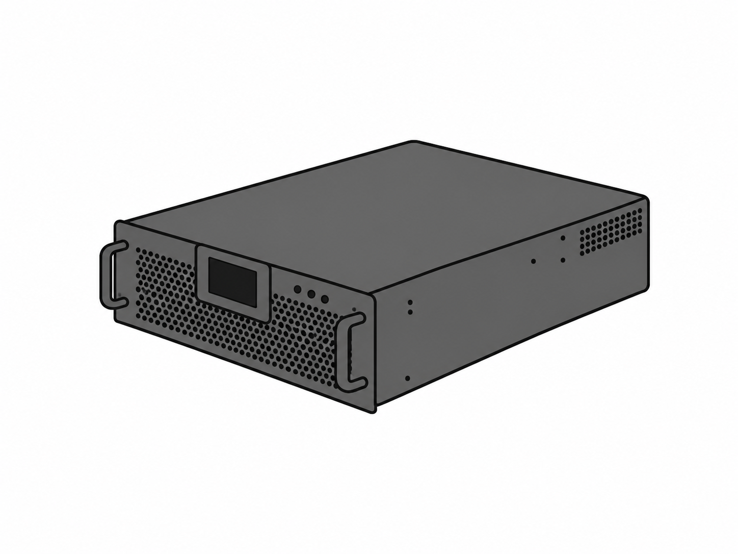
An active harmonic filter is only as good as its control loop. The filter must detect harmonic current, compute an anti-phase reference, and switch IGBTs or SiC MOSFETs before the load current has moved on — all within a fraction of a mains cycle. In CHITEK active harmonic filter design, that loop runs on an FPGA, and the choice of silicon sets the ceiling on what the loop can do. This article covers the control chain, the timing budget, why DSP-based designs fall short, and how to specify and commission an FPGA-controlled AHF alongside a static var generator.
What the Control Loop Must Do
Every AHF executes three tasks in sequence, and each one consumes time from the same budget:
- Harmonic detection — extract the harmonic content from the measured load current using FFT or instantaneous power theory (pq theory).
- Reference generation — invert that content to produce the compensation current command i_c*.
- PWM synthesis — switch the power bridge so the output current tracks i_c* within the ripple band.
The command itself is simple to state:
i_c* = i_L - i_s(fundamental)
The difficulty is that i_L changes continuously. A rectifier front end on a variable-speed drive produces a current step at every commutation, and the filter has roughly one switching period to respond before the error integrates into visible distortion.
How FPGA Control Is Quantified
The metric that matters is loop latency: the time from a change in load current to a corresponding change in filter output current. In a DSP-based design, sampling, interrupt entry, sequential computation, and PWM update typically stack into tens of microseconds. An FPGA executes the detection and reference math in parallel hardware, so latency drops to the microsecond range.
That margin is what allows the filter to track the 5th, 7th, 11th, and 13th harmonics — the dominant orders from a six-pulse rectifier — without phase lag at the switching frequency. Latency also sets the achievable control bandwidth, and bandwidth sets how fast the loop can reject a disturbance.
Major Causes of Poor Harmonic Compensation
When an AHF underperforms on site, the cause is usually one of these:
- Control latency — a slow loop leaves a residual error that shows up as elevated THDi at the PCC.
- Detection error — a PLL that loses lock during voltage distortion misidentifies the fundamental and misallocates harmonic content.
- PWM timing jitter — imprecise gate timing widens the output current ripple and wastes switching headroom.
- Saturation — the filter runs out of current capacity during load peaks and stops compensating.
- Resonance with existing capacitors — the filter and a nearby bank interact, producing amplification rather than cancellation.
What It Costs
- Utility penalties — IEEE 519 and GB/T limits on voltage and current distortion are enforced at the PCC; a residual THDi above the limit is a recurring charge.
- Transformer and cable heating — harmonic current raises I²R losses and derates capacity.
- Capacitor failure — harmonic-rich voltage accelerates dielectric aging in power factor correction banks.
- Nuisance tripping — distorted voltage confuses protection relays and drives.
Why DSP-Based Control Falls Short
A DSP runs the detection algorithm, the reference calculation, and the PWM update in sequence. Each step waits for the previous one, and each interrupt adds overhead. The result is a loop that is fast enough for slowly varying loads but lags behind a drive that switches every few hundred microseconds.
Raising the DSP clock helps only marginally, because the bottleneck is architectural, not clock speed. A faster processor still executes one instruction at a time. Moving the same math into FPGA fabric removes the serialization entirely.
How FPGA Control Fixes It
The FPGA partitions the control chain into parallel hardware blocks that all run in the same clock cycle. Detection, reference generation, and PWM comparison proceed simultaneously rather than in turn.
- Parallel detection — FFT or pq-theory blocks process all phases at once, with no shared execution resource.
- Deterministic PWM — gate signals are generated in hardware, so timing jitter is bounded by the clock, not by software scheduling.
- Closed-loop feedback — the measured output current is compared against i_c* every switching period, and the error is corrected before it accumulates.
In CHITEK active harmonic filter design, this architecture pulls THDi from 30%+ down to < 5% at the PCC, with the compensation tracking the load within < 1 ms. The same control platform drives the CHITEK SVG, where per-phase reactive current injection holds power factor at 0.99+ and rebalances negative-sequence current that a fixed bank cannot touch.
IGBT vs SiC
The control loop can only exploit the switching speed the power stage allows. Conventional IGBT-based AHF and static var generator units are capped near 150 °C junction temperature and switch typically below 20 kHz. SiC MOSFETs raise the junction limit to 200 °C, offer roughly 10× the breakdown field, and support 2-3× the switching frequency with about 50% lower switching loss.
| Parameter | IGBT stage | SiC MOSFET stage |
|---|---|---|
| Junction temperature | ~150 °C | ~200 °C |
| Typical switching frequency | < 20 kHz | 2-3× higher |
| Switching loss | Baseline | ~50% lower |
| Control bandwidth headroom | Limited | Wide |
The practical effect is a faster inner loop, a smaller output filter, and a narrower cabinet for the same compensation current. That is the direction CHITEK's LV AHF + SVG platform is built on.
Engineering Deployment Checklist
- Measure load current and PCC voltage over a full duty cycle; log the harmonic spectrum and the worst-case THDi.
- Confirm the dominant harmonic orders and size the filter current to cover them with 15-25% headroom.
- Verify the control loop latency against the fastest load step expected on site.
- Audit existing capacitor banks for resonance before commissioning.
- Check weak-grid margin and confirm the filter holds regulation through the worst-case voltage dip.
- After commissioning, re-measure THDi at the PCC against IEEE 519 and GB/T limits.
Typical Application Profiles
- Variable-speed drive clusters — commutation steps every few hundred microseconds; FPGA latency keeps the residual error small.
- Data centers — switch-mode power supplies generate broad-spectrum harmonics that need parallel detection across many orders.
- Industrial plants with mixed nonlinear load — a combined CHITEK AHF and CHITEK SVG handles both waveform distortion and reactive compensation from one control platform.
- Weak-grid feeders — fast loop response stabilizes voltage where a slow controller would oscillate.
Bottom Line
FPGA control is what lets an active harmonic filter respond within microseconds instead of milliseconds, and it is the architectural reason CHITEK active harmonic filter designs hold THDi below 5% on dynamic loads. The SiC power stage extends that advantage by widening the bandwidth the control loop can actually use. What is your worst-case load step at the PCC — and does your filter's control loop have the latency budget to track it?